Digital Logic Structures

Abstract
- Transistors
- Logic Gates
- NOT
- NOR & OR
- NAND & AND
- Combinational Logic Circuits
- Decoder
- Multiplexer
- Adder
- PLA
- Sequential Logic Circuits
- Basic Storage Elements (Latch)
- Sequential Logic Circuits Design (FSM)
- Advanced Storage Elements (Flip-Flop)
- Memory
- Address Space
- Addressability
Transistors
MOS Transistors are below the lowest level of abstraction, so we don't need to care about how they are constructed and how they work, we just need to use it to build logic gates.
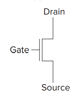
- NMOS(N-type MOS)
When NMOS is supplied with high volts, the gate acts like a wire, and drain and source are connected(short circuit).
When NMOS is supplied with low volts, the connection between drain and source is broken(open circuit).
- PMOS(P-type MOS)
The act of PMOS is exactly the opposite fashion from NMOS. High volts lead to disconnection while low volts lead to connection.
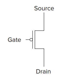
It's worth noting that whether in PMOS or NMOS there is a drain and a source, specifying the direction of the current and it can only flow from source to drain and the position of drain and source can't exchange.
Logic Gates
Now, we can build common logic gates based on P-type and N-type MOS transistors.
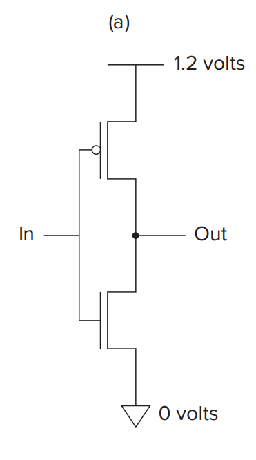
In the parts below, we use 1.2V for high volts while 0V for low volts.
NOT
The NOT gate is also called inverter and its use to negate the input. e.g. If the input is 1.2V then the output is 0V and vice versa.
The construction of the NOT gate is as followed:
NOR & OR
The NOR gate and the OR gate act like logical functions NOR and OR. You can turn to chapter 2 to review its behavior and truth table.
Here is one kind of construction of NOR gate:
Based on the NOR gate above, we can add an inverter to the output of the NOR gate then we can obatain a construction of the OR gate.
Someone may wonder why we only exchange gates above and below the output and when building the OR gate, like this:

This implementation breaks the rule that the position of source and the drain can not exchange. Thus there may be some transmission loss of voltage. (If interested, you can search for reasons on the Internet. Actually it's not what we should care about as a CS student.)
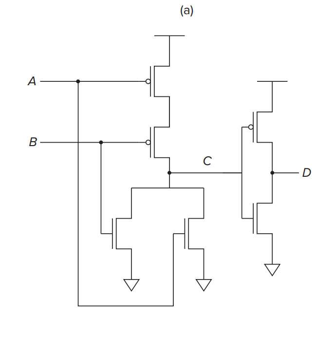
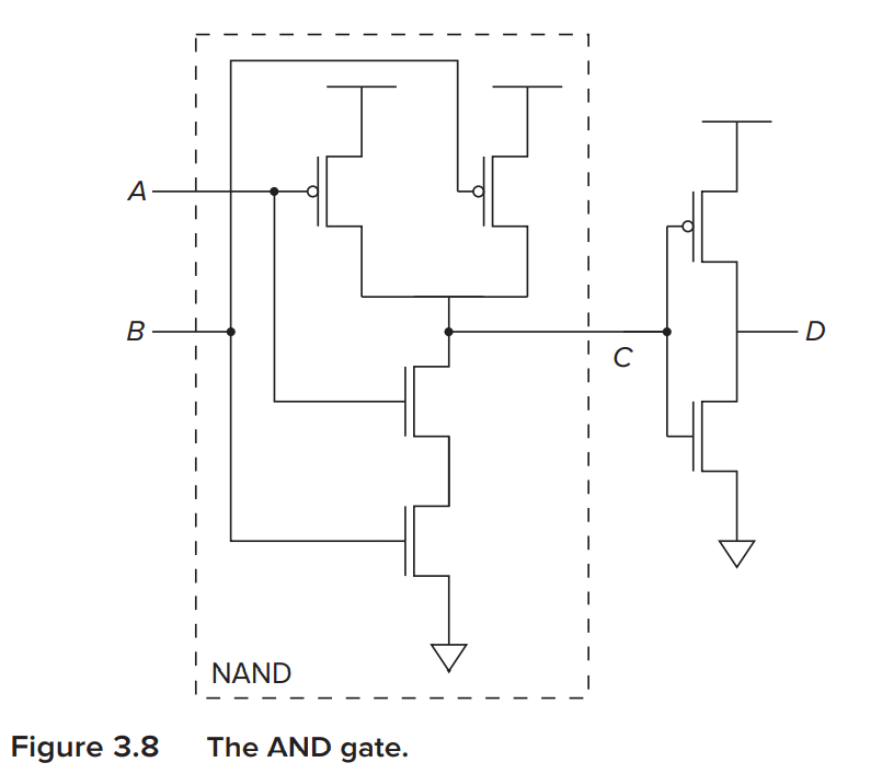
Therefore, in practice we still use 6 transistors to build a AND gate.
NAND & AND
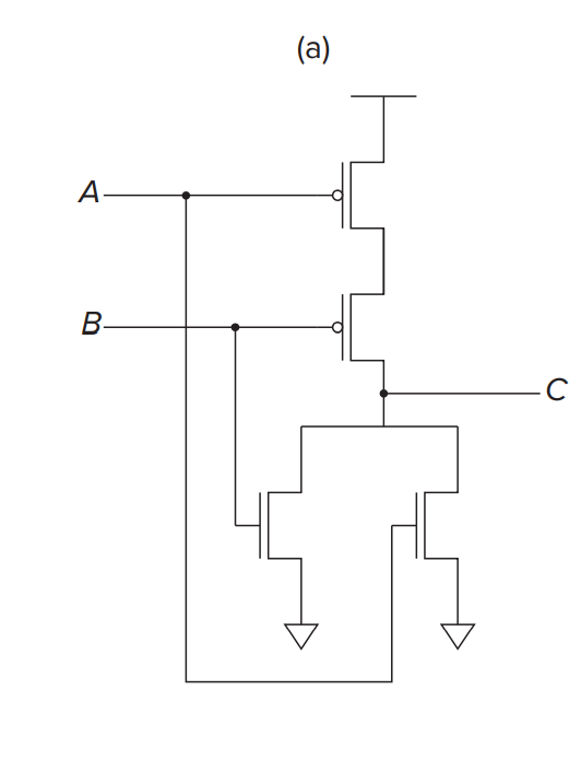
The NAND gate and the AND gate act like logical functions NAND and OR. You can turn to chapter 2 to review its behavior and truth table.
Here is a construction of the NAND and AND gate:
Summary of Logic Gates
So far, we have learned how to construct common logic gates, which means we now stand on a higher abstraction level, from transistors to logic gates. In following content, we don't need to care about the concrete construction of gates, thus we use some symbols to represent them.
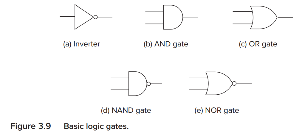
It's worth noting that a hollow circle means "NOT". e.g. You can easily find the NAND gate is the AND gate plus a hollow circle on its output.
Actully, input can also be inverted, so a hollow circle can also be used on input ports.
Besides, when there are more than 2 inputs, we also represent it as the gate with 2 inputs.
A 3-input AND gate

Although we may be more familiar with AND, OR and NOT, the universal gates are NAND or NOR. (reasons in Part 3.5)
Combinational Logic Circuits
There are fundamentally 2 kinds of logic structures, combinational and sequential. The difference between them is whether they can store information in the circuit or not.
In this part we talk about combinational logic circuits. The characteristic of it is that we can immediately determine outputs with inputs provided and outputs are not dependent on any past history of circuits at all.
Before we enter the main part, please be clear that if there is only a wire without number, then the wire only carries 1-bit data. If there is a wire with a number \(n\), then the wire carries \(n\)-bit data.
Here we talk about 3 common combinational logic circuits: Decoder, Mux and Adder.
Decoder
A decoder has \(n\) inputs and \(2^n\) outputs and only one of its outputs is 1 and all the rest are 0s.

Note that the inverter can also be added to the input port of AND gates, so 2-4 decoder can be constructed like this:
Multiplexer
The function of a multiplexer (mux for abbreviation) is to select one of the inputs and connect it to the output. The select signal determines which input is connected to the output.
2-to-1 Mux
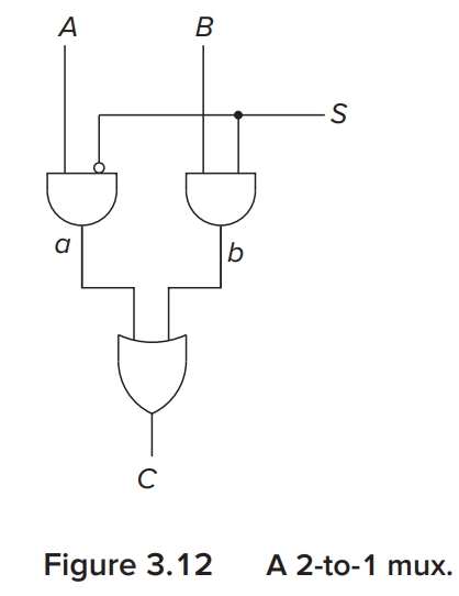
You can easily find that \(A\) will be outputed when \(S=0\) otherwise \(B\) will be outputed.
And it can be writed as a symbol like this:
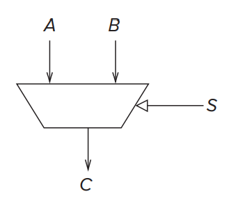
In general, a mux consists of \(2^n\) inputs, \(n\) select lines (can also be writed as 1 line with \(n\) bits) and 1 output.
Example

Adder
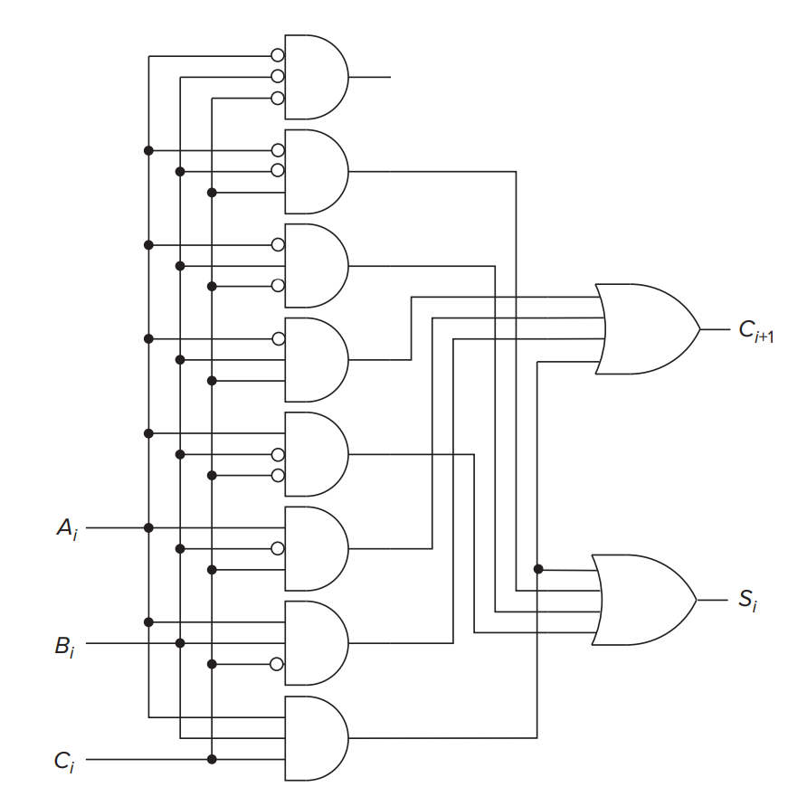
First we consider a truth table of 1-bit binary addition. We use \(A_i, B_i\) for the \(i\)-th bit of \(A, B\), the sum bit \(S_i\) for the \(i\)-th bit of the result and the carry bit \(C_{i+1}\). (\(C_i\) is the carry bit from the previous addition, \(C_{i+1}\) is the carry bit for the next addtion)
| \(A_i\) | \(B_i\) | \(C_i\) | \(C_{i+1}\) | \(S_i\) |
|---|---|---|---|---|
| 0 | 0 | 0 | 0 | 0 |
| 0 | 0 | 1 | 0 | 1 |
| 0 | 1 | 0 | 0 | 1 |
| 0 | 1 | 1 | 1 | 0 |
| 1 | 0 | 0 | 0 | 1 |
| 1 | 0 | 1 | 1 | 0 |
| 1 | 1 | 0 | 1 | 0 |
| 1 | 1 | 1 | 1 | 1 |
Here is a logic gate implementation of a 1-bit adder.
We can build a circuit for adding two 4-bit binary numbers using 1-bit adders.
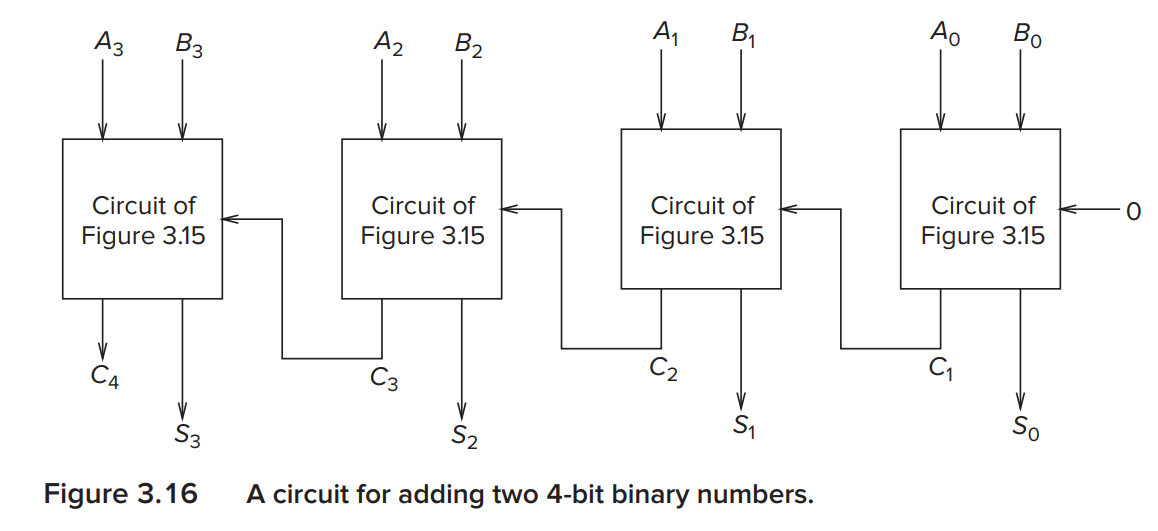
In the diagram above, the rightmost one is a half adder while the other are full adders. The difference between them is the carry bit. In the half adder \(C_i\) is default to 0 while in the full adder \(C_i\) might be 1 from previous addition.
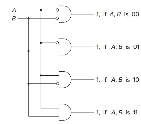
PLA
PLA (Programmable logic array) consists of an array of AND gates followed by an array of OR gates.
The common form of PLA is like this:
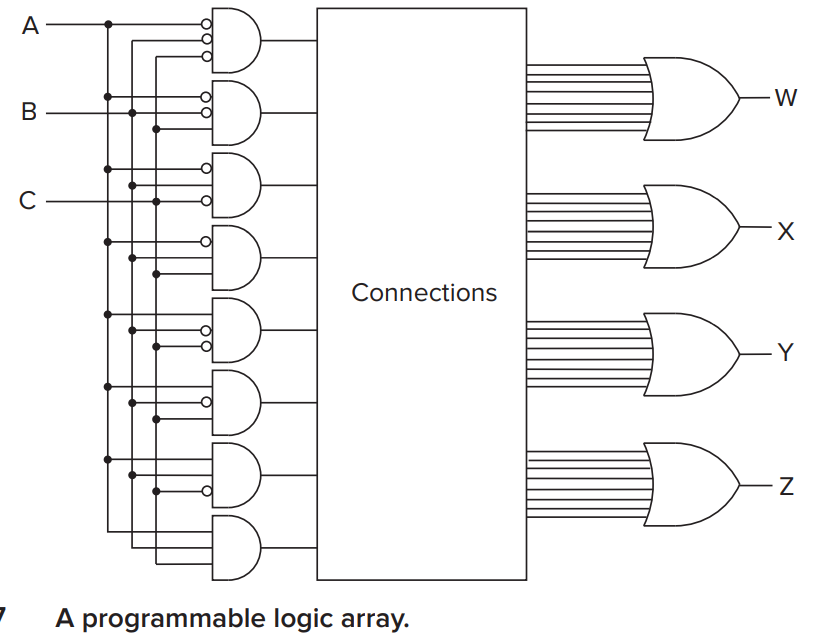
Suppose there are \(n\) logical variables (i.e. inputs) and we want to implement \(m\) logical functions(i.e. outputs). For each function, we can write the truth table for it and find combinations of variables that can make the functions output 1.
e.g. For \(W=A\cdot B\cdot C\), only when \(A=1,B=1,C=1\) that we have \(W=1\).
In PLA, we first use a decoder to get variable combination, then connect the correspounding combination of input variables to each output OR gate.
Logical Completeness
We say PLA has the property logical completeness since it can express any logic function. In PLA, we only use AND, OR and NOT gates, which means {AND, OR, NOT} is logical complete.
Remind that we say NAND gates are universal, which means NAND is also logical complete. NOR is the same. The proof is left for readers to verify.
Sequential Logic Circuits
In this part we talk about sequential logic circuits. The characteristic of it is that they contain store elements to keep track of prior history information.
So in this part we first dicuss how to store information in circuits, then we talk about how to design sequential logic circuits.
Basic Storage Elements
R-S Latch
The R-S latch can store 1 bit of information. It has two inputs \(R\) and \(S\) and two outputs \(a\) (We say this port is \(Q\)) and \(b\) (We say this port is \(\overline{Q}\)).
Since we define one port is \(Q\) and the other is \(\overline{Q}\), we can easily find that \(a=\overline{b}\) and \(b=\overline{a}\).
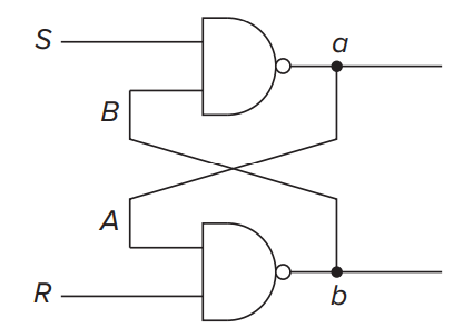
The work process is as followed:
- At beginning suppose \(S=R=1\), the latch is in chaos, we cannot know the value of \(a, b\).
- If we want to set (i.e. store 1) the latch.
We change \(S\) from 1 to 0, then \(a\) becomes 1 and \(b\) becomes 0. After that we change \(S\) back to 1, now \(S=R=1\) but the stored value will not change, which means we successfully store 1 into the latch. - If we want to reset (i.e. store 0) the lach.
We change \(R\) from 1 to 0, then \(b\) becomes 1 and \(a\) becomes 0. After that we change \(R\) back to 1, now \(S=R=1\) but the stored value will not change, which means we successfully store 0 into the latch.
Note that
- In the field of digital logic circuit, set means 1 for output while reset means 0.
- We describe the quiescent state (or quiet) of a latch as the state when the latch is storing a value, either 0 or 1. This is the case when inputs \(S=R=1\).
- If \(S=R=0\) then \(a=b=1\), disobeying the rule that \(a=\overline b\). So in practice we don't allow this input occurs.
The table below can summarize the process of the latch
| \(S\) | \(R\) | \(a(Q)\) | \(b(\overline Q)\) | |
|---|---|---|---|---|
| 1 | 1 | ? | ? | Unknown |
| 0 | 1 | 1 | 0 | Set |
| 1 | 1 | 1 | 0 | The latch "remenber" the value |
| 1 | 0 | 0 | 1 | Reset |
| 1 | 1 | 0 | 1 | The latch "remenber" the value |
| 0 | 0 | 1 | 1 | Both go to high |
| 1 | 1 | ? | ? | Unknown |
Gated D Latch
To be useful, it is necessary to control when a latch is set and when it is cleared. The gated D latch is a simple way to do this.
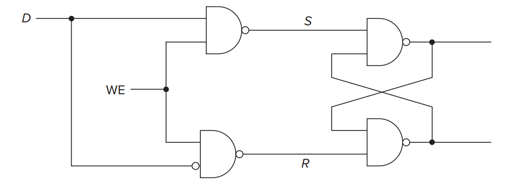
In the diagram, \(D\) is the value that we want to store into the latch. \(WE\) stands for write enable.
- \(WE\) is asserted (\(WE=1\), can write)
- \(D=1\), then \(S=0,R=1\), 1 is stored.
- \(D=0\), then \(S=1,R=0\), 0 is stored.
Thus, we can think that the Gated D Latch store the value of \(D\).
- \(WE\) is not asserted (\(WE=0\), only read)
- \(R=S=1\), so whether \(D\) is 0 or 1 it cannot change the stored value.
Sequential Logic Circuits Design
Finite State Machine
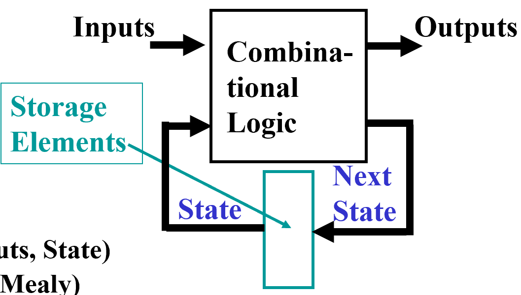
- The state of a system is a snapshot of all the relevant elements of the system at the moment the snapshot is taken.
- current state/next state
- Sequential are used to implement a very important class of mechanisms called finite state machines (FSM for abbreviation).
A finite state machine contains:- A finite number of states.
- A finite number of external inputs.
- A finite number of external outputs.
- An explicit specification of all state transitions.
- An explicit specification of what determines each external output value.
- The sequential circuit function can be represented in graphical form as a state diagram with the following components:
- A circle with the state name in it for each state
- A directed arc from the Present State to the Next State for each state transition
- A label on each directed arc with the Input values which causes the state transition, and a label:
- On each circle with the output value produced, or
- On each directed arc with the output value produced.
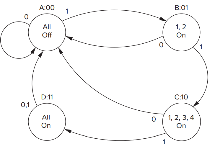
Example of FSM

There are 5 lights. At beginning, all lights are off. When the switch is in the ON position, the controller directs the lights as follows:
During one unit of time, all lights will be off. In the next unit of time, lights 1 and 2 will be on. The next unit of time, lights 1, 2, 3, and 4 will be on. Then all five lights will be on. Then the sequence repeats: no lights on, followed by 1 and 2 on, followed by 1, 2, 3, and 4 on, and so forth. Each unit of time lasts one second.
-
We can draw the state diagram for the example like this:
-
We can obtain the sequential logic circuit from the state diagram:
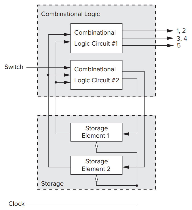
Here Storage Element 1 stores the high bit of the state name while Storage Element 2 stores the low bit.
-
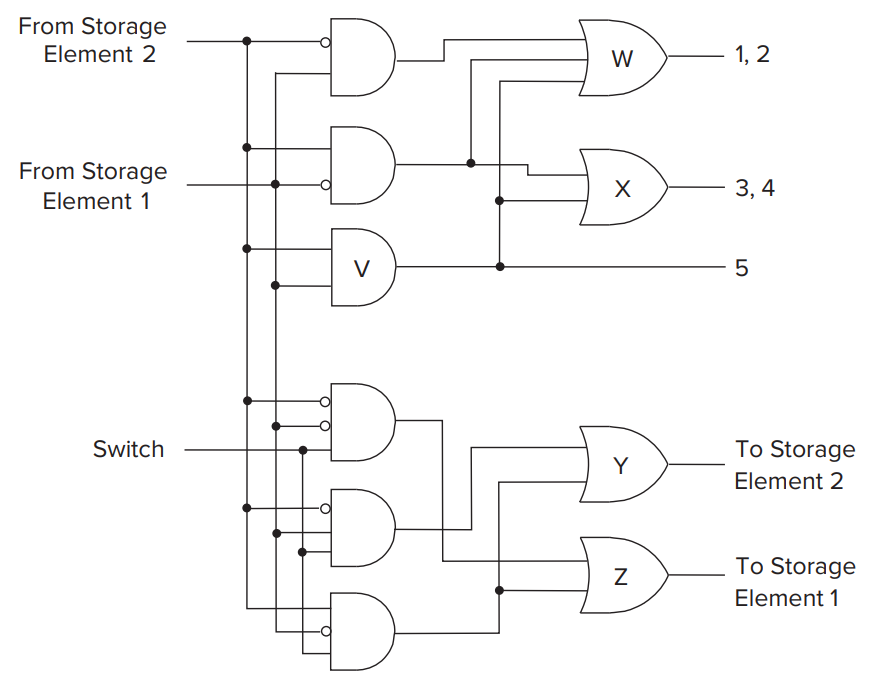
We can obtain combinational logic circuit from the state diagram.
The state transistion can be identified by the truth table. Here we use \(A(t)\) for Storage Element 1, \(B(t)\) for Storage Element 2 at time \(t\). \(A(t+1), B(t+1)\) for time \(t+1\).\(A(t)\) \(B(t)\) \(A(t+1)\) \(B(t+1)\) 0 0 0 1 0 1 1 0 1 0 1 1 1 1 0 0 So we can get the combinational circuit like this:
You can turn to textbooks for more examples of FSM.
Advanced Storage Elements
In the previous example, there is a question: The process is so fast that the input of next cyle will be the output of the last cycle almost immediately. So we have no idea what the state of the finite state machine woule be for the next clock cycle.
Actually, latches are asynchronous since if the external input changes, the stored value and the output will immediate change as well.
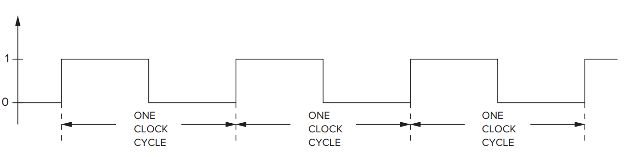
However, in practice, we usually use synchronous circuits. That is, a circuit with a clock. The clock signal alternates at a fixed time and the each of the repeated sequence of identical intervals is referred to as a clock cycle.
FSM can only make 1 state transition each clock cycle.
Therefore, we need advanced storage elements to implement synchronous storage that is, Flip-Flop.
Master-Slave Flip-Flop
A Master-Slave Flip-Flop is implemented by 2 Gated D Latch. Clock signal acts as WE signal. The right part is called slave while the left part is called master.
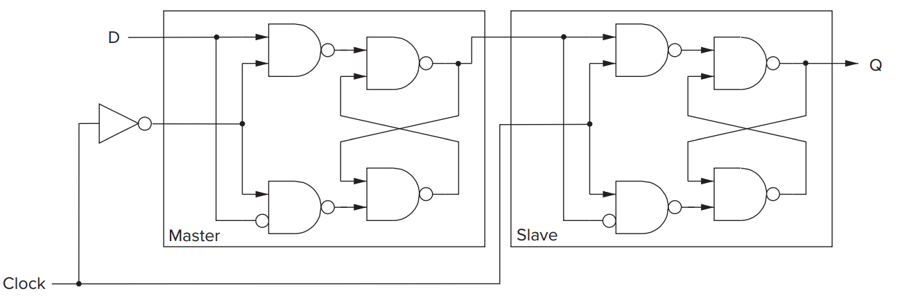
- In the first half A (i.e. \(Clock=WE=1\)), the slave read the value from the master and update the value by combinational circuits (\(Q\)) while the master remain the same.
- In the second half B (i.e. \(Clock=WE=0\)), the value updated by combinational circuit is stored in master while the slave remain the same.
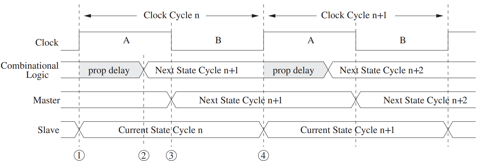
- Timing diagram
- the slave load the value from the master.
- the combinational logic finishes its update/calculation(proper delay). So it enters the next cycle.
- the master load the updated value, so it also enters the next value.
- repeat 1
Memory
Memory is made up of a number of locations, each uniquely identifiable and each having the ability to store a value.
Address Space
We refer to the unique identifier associated with each memory location as its address.
We refer to the total number of uniquely identifiable locations as the memory’s address space.
Addessability
We refer to the number of bits of information stored in each location as its addressability.
For \(2^n\)-by-\(m\)-bit memory, its address space is \(2^n\) while its addressability is \(m\).
Example
假设玉湖七幢 6 楼为一块内存,其中这一楼一共有 20 间寝室,这就是内存空间
而每间寝室都是四人间,因此可寻址能力是 4,表示最小的寻址单元。
\(2^2\)-by-3-bit Memory
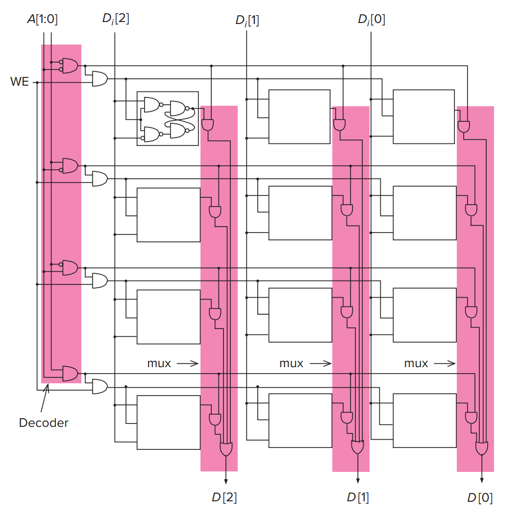
- \(A[1:0]\) is the address. So there are at most 4 locations that can store values. Given an address, decoder will tell us which location that we can access.
- Since each location has 3 flip-flops, we can store 3 bits in a location, which implies the addressability is 3 bit.
- \(WE=0\) is for reading data. \(D[i]\) is the \(i\)-th bit result. Here we use a mux to select which bit is from the address that we access.
- \(WE=1\) is for writing data. \(D_i[2:0]\) is the data that we will write into memory. Meanwhile, the reading result \(D[2:0]\) will also have outputs.
创建日期: 2023年7月5日 20:07:44